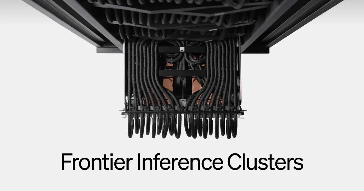
Etched raises $300 million in a new funding round valuing the AI inference chip startup at $10.3 billion, the company announced Wednesday. Sequoia Capital led the round, joined by Andreessen Horowitz, Jane Street, Diffusion, Argo, and SK Hynix. Alongside the funding, Etched disclosed a 10-megawatt lab it built 15 minutes from its San Jose office and confirmed that fabrication of hundreds of millions of dollars in inference cluster hardware is already underway.
From $5 Billion to $10.3 Billion in 23 Days
On June 30 - 23 days ago - Etched emerged from stealth at a $5 billion valuation, with $800 million in total funding and more than $1 billion in signed customer contracts. Wednesday's close more than doubles that number. Multiple reports suggest Etched is also negotiating a separate round at a $20 billion valuation that has not yet closed. SK Hynix's presence among investors is worth flagging: the South Korean company manufactures the high-bandwidth memory used in most AI accelerators, which means Etched has embedded a critical supply chain partner at the cap table level.
Two Hardware Breakthroughs Drive the Design
Etched's core argument is that frontier AI models need hardware built specifically for inference, not repurposed GPU clusters. Chips, packages, PCBs, cold plates, and interconnects get co-designed as a single system - what Etched calls a frontier inference cluster. Two breakthroughs underpin the approach: Low Voltage Inference (LVI), which runs compute blocks at under half the voltage of standard AI chips to avoid thermal throttling on trillion-parameter MoE models; and Cluster Scale Memory (CSM), a shared memory pool across chips using a proprietary ultra-low-latency interconnect that cuts the bottleneck typically imposed by HBM. Etched's first-generation A0 silicon came back from TSMC's N4P process node earlier this year and is currently in customer validation.
10-Megawatt Lab and the Fabrication Ramp
Etched built a 10-megawatt lab near its office for continuous hardware deployment, alongside a Taiwan factory, data center, and test house running out of its San Jose headquarters. "Production is the product" is how the company frames running manufacturing in parallel with engineering rather than treating it as a downstream step. OpenAI and Broadcom's Jalapeño chip targets the same LLM inference market, and Google is building the Frozen v2 chip with Gemini inference baked into the silicon - a sign of how many organizations now believe inference-optimized hardware will outperform general-purpose GPUs at scale.
Etched raises $300 million as its 400-person team - drawn from NVIDIA, Google TPUs, Broadcom, SK Hynix, and TSMC - begins fulfilling over $1 billion in customer contracts with first rack shipments expected this summer. Together AI raised $800 million in June to scale open-source inference at the software layer; Etched is placing the same bet in silicon. Neither Etched nor its investors have disclosed terms or timing for the reported $20 billion round.